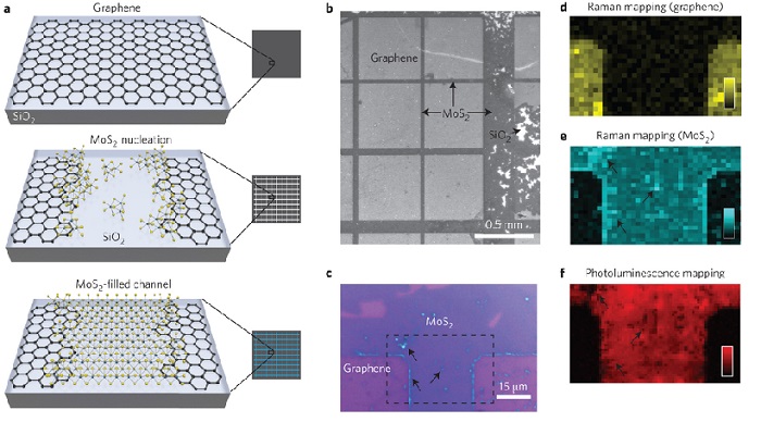
Next-generation electronics calls for new materials beyond silicon, aiming at increased functionality, performance and scaling in integrated circuits. In this respect, two-dimensional gapless graphene and semiconducting transition-metal dichalcogenides have emerged as promising candidates due to their atomic thickness and chemical stability. However, difficulties with precise spatial control during their assembly currently impede actual integration into devices. Here, we report on the large-scale, spatially controlled synthesis of heterostructures made of single-layer semiconducting molybdenum disulfide contacting conductive graphene. Transmission electron microscopy studies reveal that the single-layer molybdenum disulfide nucleates at the graphene edges. We demonstrate that such chemically assembled atomic transistors exhibit high transconductance (10 µS), on–off ratio (∼106) and mobility (∼17 cm2 V-1 s-1). The precise site selectivity from atomically thin conducting and semiconducting crystals enables us to exploit these heterostructures to assemble two-dimensional logic circuits, such as an NMOS inverter with high voltage gain (up to 70).
Nature Nanotechnology (2016) doi:10.1038/nnano.2016.115
Received 02 November 2015 Accepted 27 May 2016 Published online 11 July 2016
http://www.nature.com/nnano/journal/vaop/ncurrent/full/nnano.2016.115.html