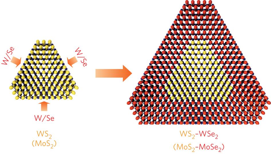
Two-dimensional layered semiconductors such as MoS2 and WSe2 have attracted considerable interest in recent times. Exploring the full potential of these layered materials requires precise spatial modulation of their chemical composition and electronic properties to create well-defined heterostructures. Here, we report the growth of compositionally modulated MoS2–MoSe2 and WS2–WSe2 lateral heterostructures by in situ modulation of the vapour-phase reactants during growth of these two-dimensional crystals. Raman and photoluminescence mapping studies demonstrate that the resulting heterostructure nanosheets exhibit clear structural and optical modulation. Transmission electron microscopy and elemental mapping studies reveal a single crystalline structure with opposite modulation of sulphur and selenium distributions across the heterostructure interface. Electrical transport studies demonstrate that the WSe2–WS2heterojunctions form lateral p–n diodes and photodiodes, and can be used to create complementary inverters with high voltage gain. Our study is an important advance in the development of layered semiconductor heterostructures, an essential step towards achieving functional electronics and optoelectronics.
Nature Nanotechnology (2014) doi:10.1038/nnano.2014.222, Advance Online Publication
http://www.nature.com/nnano/journal/vaop/ncurrent/full/nnano.2014.222.html